Table of Contents
In computer science, logic gates such as NAND gates are very useful. You can use NAND gate as universal gate. They can be helpful in designing any complex logic circuit its implementation using NAND gates only.
In this post you learn to use NAND as universal gate to create a logic diagram of a digital circuit with simple gates. If you want to learn more about logic gates visit following links.
Consider an example
Example Circuit using NAND Gates
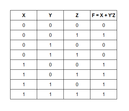
F = X + Y’Z is the given function. Show the result in truth table and draw a logic diagram using only NAND gate.
Solution:
Given function  is a Boolean function, when it receives a combination of input values, it will evaluate a single output value, based on the expression or Boolean function. This type of circuit is called a combinational circuit.
There are three variables in this function, so draw a 3 variable truth table for this function. A truth table contains all combinations of the input values of a function.
Next, if you look at the function, it is easy to determine that there are three logical operations: OR, AND, NOT. You can implement the function using a NOT gate, an OR gate and an AND gate.
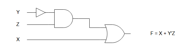
uses only two gates and an inverter – an OR gate and an AND gate. The Y input is inverted to produce Y’. The AND gate evaluate Y’Z. If the value of Y’Z is 1 or X is 1, the output of function is 1.
Convert the Logic Diagram using NAND logic gate
To convert the circuit with NOT-AND-OR circuit, you need to change the AND gate, NOT gate and OR gate to NAND equivalent. You will change AND gate with NAND gate first and then change the OR gate with NAND gate. This is shown below.
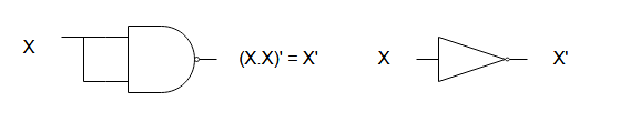
NAND gate equivalent of NOT gate
The NAND gate equivalent of inverter is created using a single NAND gate with two input X which gets inverted at the output to give X’.
The figure is function – 
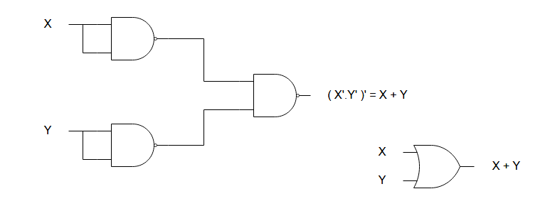
NAND gate equivalent of OR gate
The NAND gate equivalent of OR gate requires three NAND gates of which two of them invert the input values – X and Y, in this case. The output is similar to OR gate output.
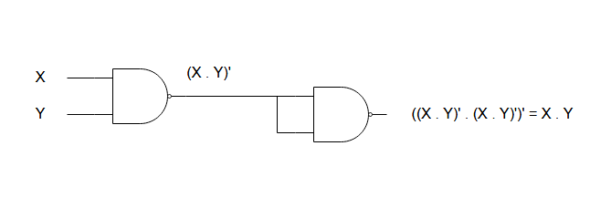
NAND gate equivalent of AND gate
The NAND gate equivalent of AND requires only two NAND gates. The first NAND produce an inverted AND output and the second NAND act as an inverter to correct the inversion and we get an AND output.
In the following diagram, you will find implementation using NAND gate only, of Boolean function  . We used
- 1 NAND for inverting Y’
- 2 NAND for AND gate with input Y’Z
- 3 NAND gates for OR gate circuit for X + Y’Z
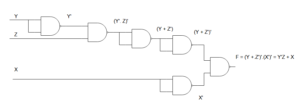
If you verify the output of the NAND gate circuit, you will find that it is same as the previous circuits created using basic logic gates. Only one type of gate is used in constructing the logic circuits which is an advantage in designing circuits.
References
- Mano, M. Morris. 1984. Digital Design. Pearson.
- NATARAJAN, ANANDA. 2015. Digital Design. PHI Learning Pvt. Ltd.