Table of Contents
Sequential Circuits have a memory element in addition to a combinational circuit so it remembers one bit of information. If a sequential circuit uses a clock pulse, then it is called “Clocked Sequential Circuit”.
There are two types of Sequential Circuits,
- Synchronous Sequential Circuits
- Asynchronous Sequential Circuits
In synchronous sequential circuits the memory or the storage element is affected only when it receives a clock pulse. Synchronization is usually achieved through a Master Clock generator which generates a periodic “Clock Pulse”.
The asynchronous sequential circuits have a feedback circuit to the input. It’s working depends on the input to the circuit and order of change in the input to the circuits. This is the reason why asynchronous sequential circuits are not stable. The memory element which store 1 bit information are Flip-Flops.
Flip-Flop Types
There are many types of flip-flop circuits.
- S-R Latch
- R-S Flip-flop
- D Flip-flop
- J-K Flip-flop
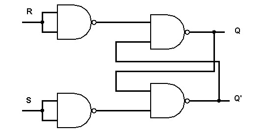
A simple flip-flop can be constructed using 2 NAND gate or 2 NOR gate. Since, NAND is a universal gate it is quite easy to implement a flip-flop circuit.
An Important thing to remember is that a flip-flop has two Output – Q and Q’. At any given time that output of Q and Q’ are complement of each other.
S-R Latch
First consider a S-R latch or S-R flip-flop , you can construct this flip-flop using NAND gates or NOR gates.
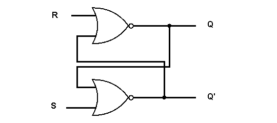
S-R Flip-Flop
S-R Flip-Flop This is a very simple implementation and there is not clock applied in this gate. I have used two NOR gates to construct this flip-flop. Let’s see how to construct using two NAND gates.
S-R Latch using Truth Table
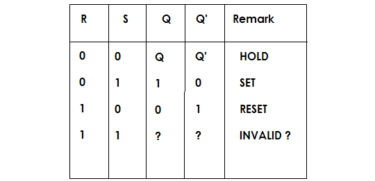
Assume that the Flip-flop is in Set state, means Q = 0 , then Q’ should be 1 because it is complement of Q.
Let’s see what happens in the NOR implementation of S-R latch.
R = 0 and S = 0,Whenever any input is 1 ,then it operates first and give output and that goes to the feedback circuit of the other gate.
Since, both are 0, nothing happens, such a state is called HOLD state.
R = 0 and S = 1,
(S + Q)' = (1 + 0)' = 0
The output of lower NOR gate is 0.
(R + Q')' = (0 + 0) = 1Output of upper NOR gate is 1 .
That means Q [Set] = 1 and Q’= 0 and flip-flop goes to SET.
R = 1 and S = 0,We already know that Q = 1 , Q’ = 0
(R + Q')' = (1 + 0)' = 0Output of upper NOR gate is 0.
(S + Q)' = (0 + 0)' = 1Output of lower NOR gate is 1 and flip-flop goes to RESET .
R= 1 and S= 1,This is undesirable, then the flop goes to an INVALID state.
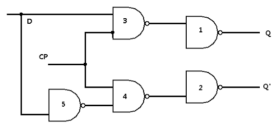
D Flip-Flop
The idea of D flip-flop is to remove the ‘Invalid’ state and make sure that the inputs are never same.
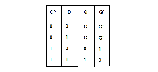
D Flip-flop has two inputs – D and CP.
When the CP =0 , then Gate 3 and Gate 4 never changes and remain in level 1, means nothing goes to the output. This happens regardless of the input at D.
If CP = 1 and D =1 , this will SET the flip-flop and Q = 1
If CP = 1 and D = 0 , this will RESET the flip-flop and Q' = 1
D Flip-flop is called this way because it holds “Data” in flip-flop and also called as Gated D-Latch.
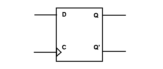
Truth Table Of D-Flip-Flop
The truth table shows that there is no invalid state as in the case of S-R flip-flop.