Simplifying Boolean Function using K-Map -Special Case
K-Map technique is a straight forward and simple method for minimizing Boolean functions. In this article, you will learn a special case of K-map, when the function is in a Standard Sum of Product and not in a Canonical Sum of Product form.
For example
F = A'B'C' + ABC'            -  (1)

F = A'B + BC' + A'B          -  (2)
In function1, each term is called a minterm( A’B’C). The sum of minterms is called a Canonical Sum of Product. It can be directly taken from the Truth Table for the function.
The function2 has terms called a product term which may have one or more literal. The sum of all such terms is called a Standard Sum of Product. The same concept applies for Canonical Product of Sum form.
Now the problem is that if you are given a standard sum of product for Boolean minimization, what to do, because it appears that its already minimized.
How to simplify the function ( 2 )using K-Map?
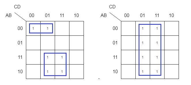
Create a three variable map like we do always .and put 1 in the box where a particular term is missing .
A'BWhich term is missing? yes right! it’s C
A'B( C + C')
A'BC + A'BC'
In the map you put 1 in the cell for both
A'BC + A'BC'Similarly, Solve other missing variable in each of the terms of the function.
Now, you can minimize the above 3-variable K-Map easily because you have identified the correct boxes.
Subtraction using 10’s complement
In digital computer systems, arithmetic operations are simplified using the radix complement system also known as r’s complement system. The r stands for radix which is a base for a number in a particular number system. In this post, you learn to do subtraction using 10’s complement.
You must be familiar with the complement system in digital logic to understand this subtraction method. To learn about complements visit the following link.
Examples of number system are decimal, binary, octal, hexadecimal. In a binary system we have complements.
For example,
If you talk about a binary system, the base is 2, then we have two types of r’s complement.
- r’s complement
- (r-1)’s complement
For decimal number the r’s complement is 10’s complement and (r-1)’s complement is 9’s complement because base is 10. In other words, decimal number has base r = 10, so 10’s complement and r-1 = 9, so 9’s complement. The binary number has base r = 2, 2’s complement and r-1 = 1 , so one’s complement.
Q1. Subtract using 10’s complement 52 – 12 .
We know that 52 – 12 = 40
Let m = 52 and n = 12
Take 10’s complement of 12
\begin{aligned}
&+99\\
&-12\\
&----\\
&+87
\end{aligned}
Now, 87 is 9’s complement because we subtracted it with 99. To make it 10’s complement add 1 to 87. The 10’s complement of 12 is 88. Add the 88 to m
\begin{aligned}
&+52\\
&+88\\
&----\\
&\hspace{8px}140
\end{aligned}
Answer: Remove the extra 1 and you get 40
Check the second example.
Q2: Subtract using 10’s complement 12 – 52
We know that 12 < 52, so answer is -40
Let m = 12 and n = 52
10’s complement of 52
\begin{aligned}
&+99\\
&-52\\
&----\\
&+47
\end{aligned}
The 9’s complement of 52 is 47. To make it 10’s complement add 1 to 47.
Add 48 to m
\begin{aligned}
&+12\\
&+48\\
&----\\
&+60
\end{aligned}
This is not the answer , wait
Take one more 10’s complement of the result.
\begin{aligned}
&+99\\
&-60\\
&----\\
&+39
\end{aligned}
The 9’s complement of 60 is 39. Add 1 to 39 and make is 10’s complement.
Add negative to the result because m > n.
Answer: -40
Summary
How do I take 10’s complement ?
Suppose n = 123 then
There are 3 digits in 123. The 10’s complement would be 9’s complement + 1.
\begin{aligned}
&999 - 123 = 876\\
&876 + 1 = 877
\end{aligned}
Therefore, the 10’s complement of 123 is 877.
References
- John.F.Wakerly. 2008. Digital Design: Principles And Practices, 4/E. Pearson Education, India.
- Mano, M. Morris. 1984. Digital Design. Pearson.
Sequential Circuits – Flip Flop Circuits
Sequential Circuits have a memory element in addition to a combinational circuit so it remembers one bit of information. If a sequential circuit uses a clock pulse, then it is called “Clocked Sequential Circuit”.
There are two types of Sequential Circuits,
- Synchronous Sequential Circuits
- Asynchronous Sequential Circuits
In synchronous sequential circuits the memory or the storage element is affected only when it receives a clock pulse. Synchronization is usually achieved through a Master Clock generator which generates a periodic “Clock Pulse”.
The asynchronous sequential circuits have a feedback circuit to the input. It’s working depends on the input to the circuit and order of change in the input to the circuits. This is the reason why asynchronous sequential circuits are not stable. The memory element which store 1 bit information are Flip-Flops.
Flip-Flop Types
There are many types of flip-flop circuits.
- S-R Latch
- R-S Flip-flop
- D Flip-flop
- J-K Flip-flop
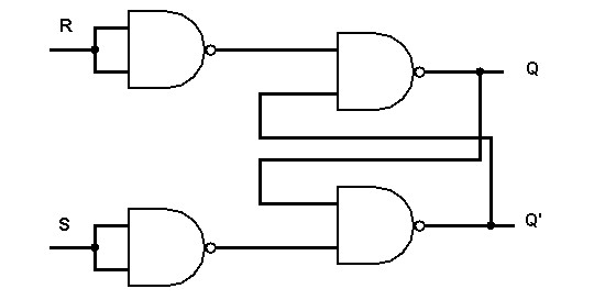
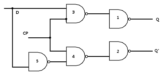
A simple flip-flop can be constructed using 2 NAND gate or 2 NOR gate. Since, NAND is a universal gate it is quite easy to implement a flip-flop circuit.
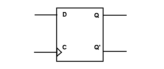
An Important thing to remember is that a flip-flop has two Output – Q and Q’. At any given time that output of Q and Q’ are complement of each other.
S-R Latch
First consider a S-R latch or S-R flip-flop , you can construct this flip-flop using NAND gates or NOR gates.
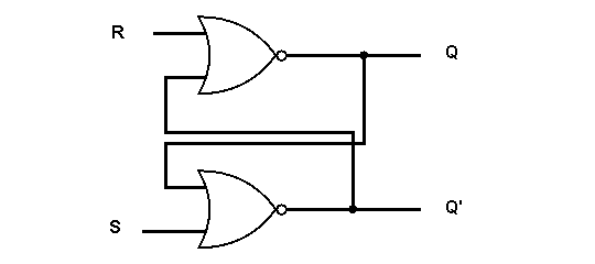
S-R Flip-Flop
S-R Flip-Flop This is a very simple implementation and there is not clock applied in this gate. I have used two NOR gates to construct this flip-flop. Let’s see how to construct using two NAND gates.
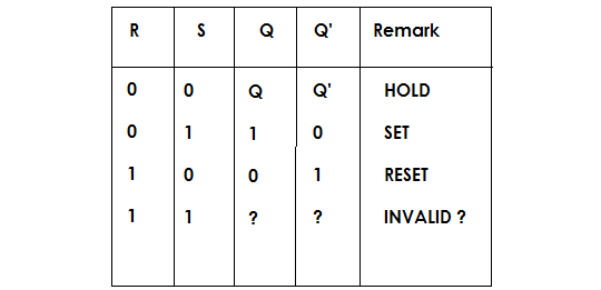
S-R Latch using Truth Table
Assume that the Flip-flop is in Set state, means Q = 0 , then Q’ should be 1 because it is complement of Q.
Let’s see what happens in the NOR implementation of S-R latch.
R = 0 and S = 0,Whenever any input is 1 ,then it operates first and give output and that goes to the feedback circuit of the other gate.
Since, both are 0, nothing happens, such a state is called HOLD state.
R = 0 and S = 1,
(S + Q)' = (1 + 0)' = 0
The output of lower NOR gate is 0.
(R + Q')' = (0 + 0) = 1Output of upper NOR gate is 1 .
That means Q [Set] = 1 and Q’= 0 and flip-flop goes to SET.
R = 1 and S = 0,We already know that Q = 1 , Q’ = 0
(R + Q')' = (1 + 0)' = 0Output of upper NOR gate is 0.
(S + Q)' = (0 + 0)' = 1Output of lower NOR gate is 1 and flip-flop goes to RESET .
R= 1 and S= 1,This is undesirable, then the flop goes to an INVALID state.
D Flip-Flop
The idea of D flip-flop is to remove the ‘Invalid’ state and make sure that the inputs are never same.
D Flip-flop has two inputs – D and CP.
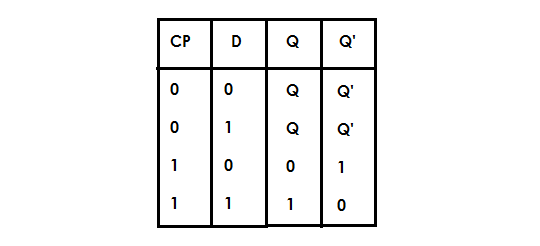
When the CP =0 , then Gate 3 and Gate 4 never changes and remain in level 1, means nothing goes to the output. This happens regardless of the input at D.
If CP = 1 and D =1 , this will SET the flip-flop and Q = 1
If CP = 1 and D = 0 , this will RESET the flip-flop and Q' = 1
D Flip-flop is called this way because it holds “Data” in flip-flop and also called as Gated D-Latch.
Truth Table Of D-Flip-Flop
The truth table shows that there is no invalid state as in the case of S-R flip-flop.
Adders
The adder is a combinational circuit that add binary digits for arithmetic computation. A combinational circuit is a kind of digital circuit that has an input, a logic circuit and an output.
For  variables, there are
  combinations of input variables and for each input combination, there is one and only one output. Therefore, output from combinational circuit is a Boolean function expressed in terms of input variables. Remember that there is only one output for an input combination.
This article we talk about adders, so you must be familiar with following concepts: Minterm, Boolean function minimization, K-map and Truth tables.
To learn about logic gates, visit following links
Binary addition
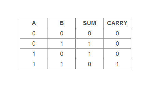
The most basic function of a digital computer is to add binary digits to perform arithmetic operations like humans do, except that we use decimal number system. A digital computer uses binary number. Suppose, you want to add two binary digits – A and B, where A and B represents 0 or 1.
If A = 0 and B = 0, then sum = 0 + 0 = 0
If A = 0 and B = 1, then sum = 0 + 1 = 1
If A = 1 and B = 0, then sum = 1 + 0 = 1
If A = 1 and B = 1, then sum = 1 + 1 = 0 and carry = 1
When the inputs are two binary digits. It produce at most two output.
- A sum
- A carry (the last operation above results in a carry)
Adders
Binary addition is the motivation behind the adder circuit and there are many types of adder circuits. There are two type of basic adders that help to build complex circuits.
- Half adder
- Full adder
Half Adder
The half adder circuit perform 2 bit addition. The two bit addition produce output called a Sum and a Carry. The outputs are binary functions, the functions of sum and carry helps in designing a logic circuit for half adder. The process of deriving a function and circuit design in given below.
Half Adder Truth Table
The truth table of half-adder shows all combinations of its input values which is  rows. Each row represents a single combination. The 2 columns are for input variables – A and B and the other two columns are for outputs: Sum and Carry.
Logic functions
The logic functions are for the output of a combinational circuit. You will derive a logic function for half-adder circuit using truth table. The process of deriving logic function is
Step 1: Select all the rows from truth table that result in 1 in sum column or carry column.
Step 2: Create a sum of product function using the minterms you obtained in step 1.
Step 3: Minimize the Boolean function obtained to get the minimum sum of product function for the output sum and carry.
For example
Step 1:
A'B, AB' for sum;
A.B for carry.

Step 2:
Sum = A'B + AB'
Carry = A.B

Step 3:
K-MAP to minimize the Boolean function.
Draw two variable maps for sum and carry using the Boolean functions. Mark the cell as 1 if it corresponds to a minterm in the respective map.
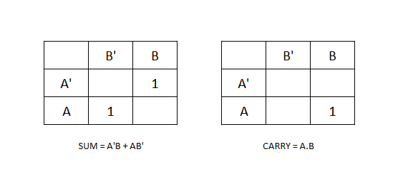
The given functions are mapped into the K-maps, but cannot be minimized because the 1s cannot be grouped, therefore, the final function is
Sum = A ⊕ B
Carry = A . B
Logic Symbol – Half Adder
Sometimes drawing complex circuit such as a 4 bit adder, needs many components and a detailed diagram for each component is not necessary. This may add to complexity. You can use a logic symbol instead to simplify things. A logic symbol for half adder is given below.
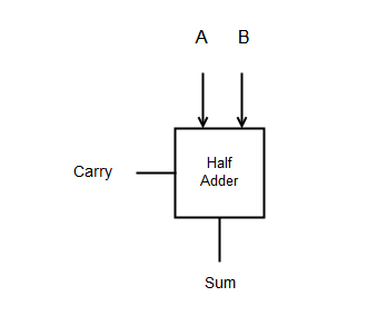
The logic diagram shows all the features of a half adder such as inputs and sum and carry. Any other details is not necessary if you are using many such adders.
Half Adder Logic Circuit
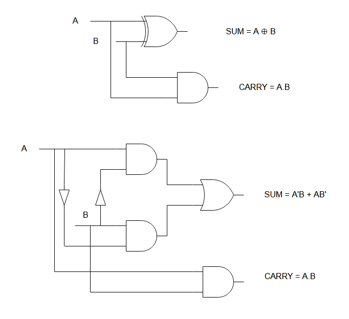
The output functions for sum and carry are the basic for designing a logic circuit for half adder circuit. Take a look at the function
Sum = A'B + AB'
Carry = A.B
You can clearly tell that the sum needs two AND gate and an OR gate to represent this circuit in real world. Similarly, Carry need a single and gate. You should note that the sum function is nothing but XOR function, so you can still minimize the number of gates by using one XOR gate and an AND gate to represent a half adder circuit.
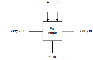
Full Adder
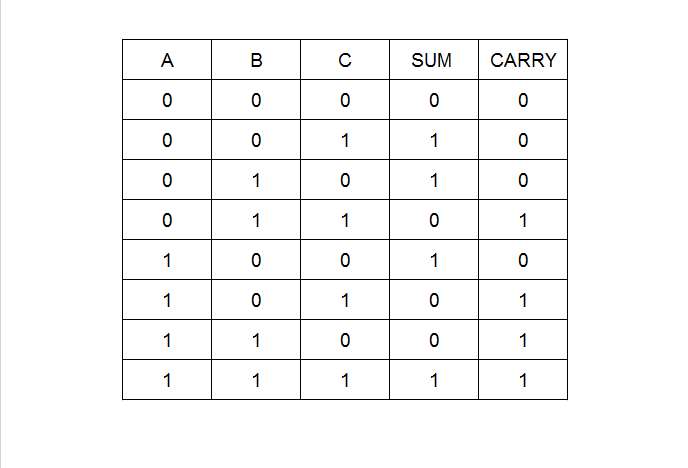
Full adder is another type of adder that adds 3 binary bits. It has 3 inputs and 2 output – Sum and Carry-out.
Three-bit binary addition
A three-bit binary addition or more is required in some digital circuits. In this case, the first two bits are evaluated first and then the result is evaluated with the third variable. See the example below.
(0 + 0) + 0 = 0
(0 + 0) + 1 = 1
Full Adder Truth table
The truth table of full adder has 3 columns for input variables and 2 columns for output. The total combinations of input variables give the number of rows which is  rows.
rows.
Logic functions
Similar to half-adder, you can derive the logical functions for outputs of a full adder using the truth table. You need to follow the same process as in the case of half adder.
Step 1: list all the minterms that has 1 as result for sum.
Step 2: Make a sum of product equation using the minterms.
Sum = A'B'C + A'BC' + AB'C' + ABC
Carry = A'BC + AB'C + ABC' + ABC
Step 3: Use K-Map to minimize the equation for sum and carry. While using the K-Maps for full adder, you may observe that the carry function can be grouped and minimized and the resulting functions are
Sum = A'B'C + A'BC' + AB'C' + ABC = A ⊕ B ⊕ C
Carry = A'BC + AB'C + ABC' + ABC = AC + AB + BC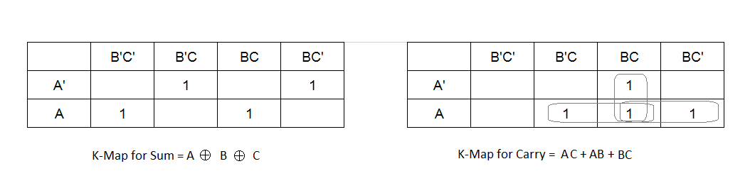
Logic Symbol – Full Adder
The logic diagram of full adder is not different from the logic diagram of the half-adder, except that one of the input of a full adder is Carry In and one output is Carry Out.
Full Adder Logic Circuit
The logic diagram is derived from the equation of outputs. The equation shows that you need two XOR gate and an OR gate. Also, you can represent the circuit using four AND gates and a single OR gate for sum and three AND gates with a single OR gate for carry.
Sum = A'B'C + A'BC' + AB'C' + ABC
Carry = BC + AC + AB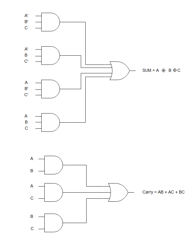
In the next article, you will learn about more complex adders such as 4 bit adder, n-bit parallel adder and so on.
References
- Mano, M. Morris. 1984. Digital Design. Pearson.
- Shjiva, Sajjan G. 1998. Introduction to Logic Design. New York: Marcel Dekker, Inc .
Combinational Circuit – Questions/Solutions
In this post, you will learn example problems from combinational circuits. These problems help in minimizing Boolean functions and constructing logic circuit diagrams. The solution to the problems are given in step-by-step manner with explanation wherever possible.
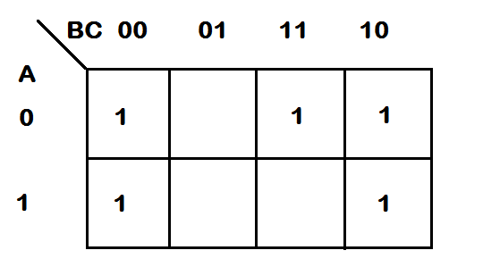
Q1. Simplify the Boolean function using K-MAP technique.
F(A,B,C,D) = Σ( 0,1,4,8,9,10)There are 4 variables in this function. First, we construct a Truth Table for four variable functions. We can see that there are 16 minterm  of which following gives a output value of 1.
Solution:
Σ( 0,1,4,8,9,)

= m0 + m1 + m4 + m8 + m9 + m10

= A'B'C'D' + A'B'C'D + A'BC'D' + AB'C'D' + AB'C'D + AB'CD' 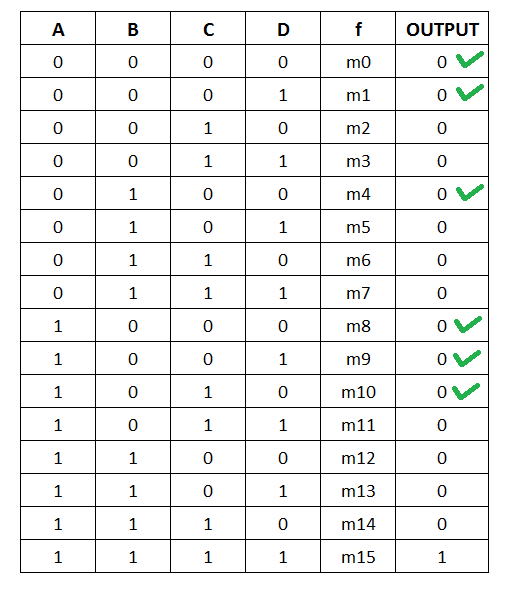
But you want the minimized Boolean function.
K-Map is great technique to reduce the minimize the Boolean function. Those minterms that give 1 is marked in the 4-variable K-map. Next, we need to group the adjacent 1s into group of 2, 4 and 8.Once grouped you can minimize the function using following method.
- Eliminate any common variable that negate each other – row wise or column wise (e.g.,
 because
- After elimination a group of two adjacent 1s will give 3 variables term(e.g.,
 ).
). - After elimination a group of four adjacent 1s will give 2 variable term (e.g.,
 ).
). - Aftter elimination a group of eight adjacent 1ss will give 1 variable (e.g,
 ).
).
 because
 ).
). ).
). ).
).Group 1 = A'B'C'D' + A'B'CD' = A'B'D'
Group 2 = A'B'C'D' + AB'C'D' + ABC'D' + A'BC'D'
= B'C'D' + BC'D'
= C'D'
Group 3 = AB'C'D' + AB'C'D' = AB'C'we have found 3 minimized minterms of our function.
= A'B'C' + A'D' + C'DB'Q2. Construct Logic Diagram of the following function using XOR and AND gates only,
F = A.B'CD' + AB'CD' + A.B'C'D + A'BC'D Solution:
F = (C.D')(A.B' + B'A) + (C'D)(A.B' + B.A')
F = (C.D')(A ⊕ B) + (C'D)(A  ⊕ B)
F = (C.D' + C'D) (A  ⊕ B)
F = (C ⊕ D) (A ⊕ B)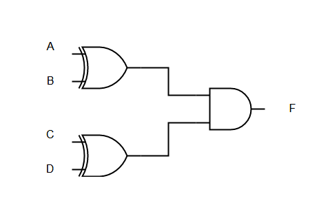
Q3. Draw the logic diagram corresponding to the following Boolean expression without simplifying them.
F=BC' + AB + ACD
F = (A + B) (C + D')(A' + B + D)
Solution: (a)
F=BC' + AB + ACD 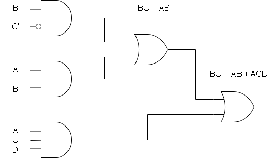
Solution: (b)
F = (A + B) (C + D')(A' + B + D)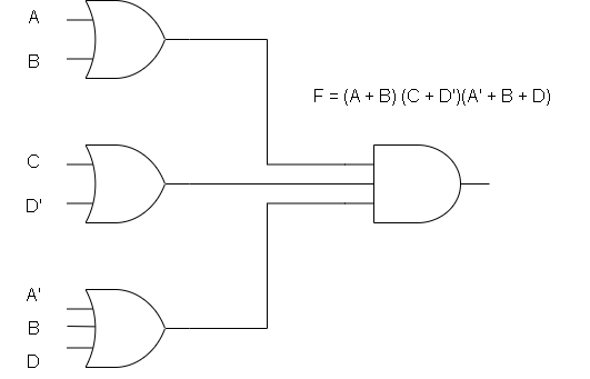
Q4. Express in Sum of Minterm and Product of Maxterm
F(x,y,z) = (x.y + z)(x.z + y)Solution:
F (x,y, z) = (x.y + z) (x.z + y)
=(x + z)(y + z)(x + y)(z + y)
=(x + z)+(y . y') . (y + z ) + ( x . x') . ( x + y )+ (z . z').(z + y)+( x . x' )
=( x + y + z).(x + y' + z).(y + z + x).(y + z + x').(x + y + z).(x + y + z').(z + y + x).(z + y + x')
=  (x + y + z) . (x + y' + z) . (x' + y + z) . (x . y . z')
= M0 . M2 . M4 . M1
Π( 0,1,2,4) [ Product of maxterm form]
F = ∑(3 , 5, 6, 7) [ Sum of Product form]
Q5. Express the complement of the function in terms of minterms.
a) F(A,B,C,D) = ∑(0,2,6,11,13,14).
b) F(x,y,z) =  Π(0,3,6,7)
Solution:
 a) F(A,B,C,D) = ∑(0,2,6,11,13,14)
= m0 + m2 + m6 + m11 + m13 + m14
Complement of F is F' and it contains those minterms not there in F. Also this is a 4 variable function to there are 24  = 16 minterm
So, F' = m1 + m3 + m4 + m5 + m7 + m8 + m9 + m12 + m15

F' = ∑(1,3,4,5,7,8,9,12,15)Understanding Sum of Minterms and Product of Maxterms
A Boolean function is expressed in two form.
- Sum of Minterms
- Product of Maxterms
Sum of Minterms
x’ y’ z , x y’ z’ , x y’ z , x y z’ , x y z , gives 1 as output in the above Truth Table.
- Literal – x, y, A, b etc is a label which denote an input variable for a logic gate. Literal can be normal or complimented.
- Minterm – product of two or more literal using ANDing of each literal.
- Maxterm – sum of two or more literal using ORing of each literal.
Before we understand what sum of minterm or product of maxterm is, we must understand a few terminology.
For example,
x or x', y or y'For example,
x.y.z or x'ySuppose we have 2 variable – x and y, then all possible combination of literals are x’y’ , x’y, xy’, xy. If we have 3 variables then all combination of literals are as follows.
Basically, if there are n variable, then there is 2^n. For 3 variable, there are 2^3 = 8.
A minterm is the term from table given below that gives 1 output.Let us sum all these terms,
F = x' y' z + x y' z'  + x y' z + x y z' + x y z
= m1 + m4 + m5 + m6 + m7
F(x,y,z) = ∑(1,4,5,6,7) is known as Sum of Minterms Canonical Form.
Why is it called canonical form ? because all the literals present in each of the terms.
Product of Maxterm
The Product of Maxterm is complement of the Sum of Minterm of a function. To obtain the Product of Maxterm, we need two step process.
- Find those minterms in the Truth Table that gives a 0 as output.
- Complement those minterms using DeMorgan’s law.
Let us now apply the above to obtain the Product of Maxterm form.
From the previous truth table given, x’ y’ z’, x’ y z’, x’ y z gives output as 0.
F = x' y' z' + x' y z' + x' y z             by Rule 1
= (x' y' z' + x' y z' + x' y z)'            by DeMorgan's Law
= (x + y + z)(x + y' + z)(x + y' + z')      Product of Maxterms form
We see that the Product of Maxterm is ANDing of all ORed terms.
Complement of a Boolean Function
The function is F and it’s complement is F’. Suppose there is a function as follows
F = x' y z' + x' y' z
We can find the complement of the function using two rule stated by DeMorgan’s Law.
- Change the OR gates with AND gates or change the AND gates with OR gates.
- Change each literal of the function with it’s complement.
Now, we will apply the above two principle in F to obtain F’.
F'= (x' y z' + x' y 'z)'

       = (x + y' + z).(x + y + z')
Consider more examples,
F = x y' + x' y

F' = (x y' + x' y)

   = (x' + y).(x + y)

Source: Digital Logic and Computer Design by Morris Mano
F  = (AB' + C)D' + E

F' = ((AB' + C)D' + E)'

   = ((AB' + C)' + D)(E')

   = ((A' + B ) . C') + D).(E')

   = (A' + B + D)(C' + D).(E')

Source: Digital Logic and Computer Design by Morris Mano
F  = (x + y' + z)(x' + z')(x + y)

F' = ((x + y' + z)(x' + z')(x + y))'

   = ((x + y' + z)' + (x' + z')' + (x + y)')'

   =((x' y z')+(x z) + (x' y'))

   = x' y z' + x z + x' y'

Source: Digital Logic and Computer Design by Morris Mano
Universal Gates
In computer science, logic gates such as NAND gates are very useful. You can use NAND gate as universal gate. They can be helpful in designing any complex logic circuit its implementation using NAND gates only.
In this post you learn to use NAND as universal gate to create a logic diagram of a digital circuit with simple gates. If you want to learn more about logic gates visit following links.
Consider an example
Example Circuit using NAND Gates
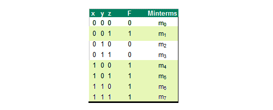
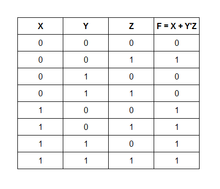
F = X + Y’Z is the given function. Show the result in truth table and draw a logic diagram using only NAND gate.
Solution:
Given function  is a Boolean function, when it receives a combination of input values, it will evaluate a single output value, based on the expression or Boolean function. This type of circuit is called a combinational circuit.
There are three variables in this function, so draw a 3 variable truth table for this function. A truth table contains all combinations of the input values of a function.
Next, if you look at the function, it is easy to determine that there are three logical operations: OR, AND, NOT. You can implement the function using a NOT gate, an OR gate and an AND gate.
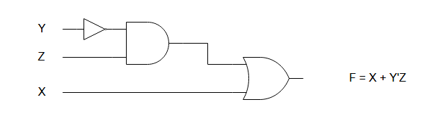
uses only two gates and an inverter – an OR gate and an AND gate. The Y input is inverted to produce Y’. The AND gate evaluate Y’Z. If the value of Y’Z is 1 or X is 1, the output of function is 1.
Convert the Logic Diagram using NAND logic gate
To convert the circuit with NOT-AND-OR circuit, you need to change the AND gate, NOT gate and OR gate to NAND equivalent. You will change AND gate with NAND gate first and then change the OR gate with NAND gate. This is shown below.
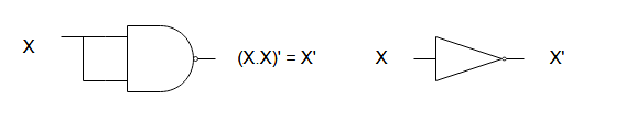
NAND gate equivalent of NOT gate
The NAND gate equivalent of inverter is created using a single NAND gate with two input X which gets inverted at the output to give X’.
The figure is function – 
NAND gate equivalent of OR gate
The NAND gate equivalent of OR gate requires three NAND gates of which two of them invert the input values – X and Y, in this case. The output is similar to OR gate output.
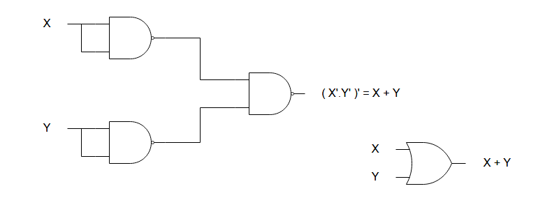
NAND gate equivalent of AND gate
The NAND gate equivalent of AND requires only two NAND gates. The first NAND produce an inverted AND output and the second NAND act as an inverter to correct the inversion and we get an AND output.
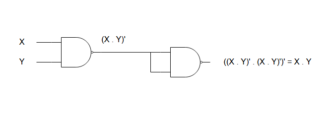
In the following diagram, you will find implementation using NAND gate only, of Boolean function  . We used
- 1 NAND for inverting Y’
- 2 NAND for AND gate with input Y’Z
- 3 NAND gates for OR gate circuit for X + Y’Z
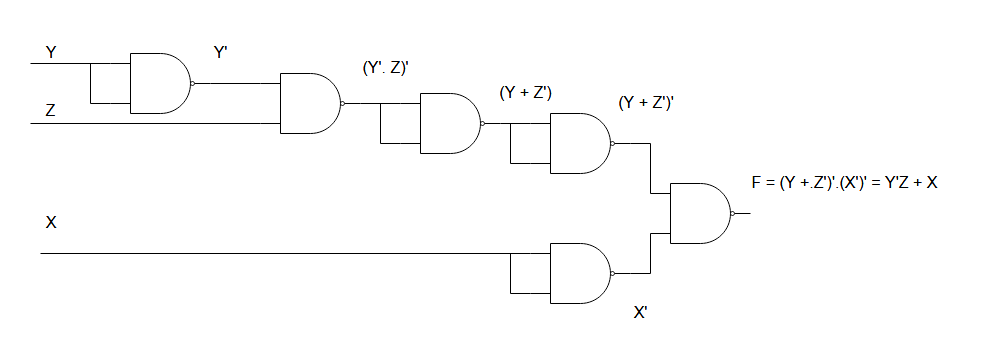
If you verify the output of the NAND gate circuit, you will find that it is same as the previous circuits created using basic logic gates. Only one type of gate is used in constructing the logic circuits which is an advantage in designing circuits.
References
- Mano, M. Morris. 1984. Digital Design. Pearson.
- NATARAJAN, ANANDA. 2015. Digital Design. PHI Learning Pvt. Ltd.
Subtraction of signed binary numbers using 2’s Complement
In this article, we will perform a subtraction using 2’s complement. An unsigned binary number does not have a sign bit in the most significant bit (MSB) position. For example, consider 8-bit representation of 3810
\begin{aligned}
&38_{10} = 0010110_2\\\\
&=0 \cdot 2^7 + 0 \cdot 2^6 + 1 \cdot 2^5 + 0 \cdot 2^4 + 0 \cdot 2^4 + 0 \cdot 2^3 + 1 \cdot 2^2 + 1 \cdot 2^1 + 0 \cdot 2^0\\\\
&= 0 + 0 + 32 + 0 + 0 + 4 + 2 + 0\\\\
&=32 + 6\\\\
&=38_{10}\end{aligned}
Now, if we take two’s complement of unsigned binary number then we get signed binary representation of a number which is nothing but negative equivalent the unsigned binary number.
To understand this in an easy way, consider previous example of 3810. Let us convert the number 3810 into binary.
38_{10} = 0 0 1 0 0 1 1 0Take 1’s complement of each binary digit in above number. That is, 0 becomes 1 and 1 becomes 0.
1's \hspace{3px} complement \hspace{3px} of \hspace{3px} 38 = 1 1 0 1 1 0 0 1Adding 1 to the 1’s complement of 3810 we get two’s complement of the binary number.
\begin{aligned}
&\hspace{1cm}1\\
&1 1 0 1 1 0 0 1\\
& +\hspace{21px}1\\
&---------\\
& 1 1 0 1 1 0 1 0
\end{aligned}
The Most Significant Bit (MSB) has 1 which shows that it is a negative number. The resultant number is -3810
Subtraction using 2’s Complement of unsigned binary number
Two’s complement of binary number is used for subtraction between unsigned and signed binary numbers.
For example,
How do we subtract? -34 – (-45) = -34 + 45 = 11
Step 1: Convert +34 in 2’s Complement form.
34 = 0 0 1 0 0 0 1 0
Obtain 1’s complement of 0 0 1 0 0 0 1 0
\begin{aligned}
&0 0 1 0 0 0 1 0\\
&+\hspace{21px}1\\
&-----\\
&0 0 1 0 0 0 1 1 = -34_{10}
\end{aligned}
Note: The above step is only performed to obtain the -34 values. There are other methods to obtain negative signed values
Step 2: Convert -45 into 2’s complement to find +45.
But we can also do it directly.
\begin{aligned}
&45 = 0 0 1 0 1 1 0 1\\
&= 0. 2^7 + 0. 2^6 + 1. 2^5 + 0. 2^4 + 1. 2^3+ 1. 2^2 + 0. 2^1 + 1. 2^0\\
&= 0 + 0 + 32 + 0 + 8 + 4 + 0 + 1\\
&= 32 + 8 + 4 + 1\\
&=45
\end{aligned}
Step 3: Add binary value of -34 and 45
\begin{aligned}
&1 1 0 1 1 1 1 0   = -34\\
& 0 0 1 0 1 1 0 1   = +45\\
&----------\\
&0 0 0 0 1 0 1 1 = 1 1 _{1 0}

\end{aligned}
Example Problems
Q 1: Perform the subtraction with the unsigned binary numbers by taking the 2’s complement of the subtrahend.
Source: Computer System Architecture by Morris Mano
a) 1 1 0 1 0 – 1 0 0 0 0
Solution:
Given
\begin{aligned}
&0001 1 0 1 0 = + 26\\
&0001 0 0 0 0 = + 16\\\\
&Take \hspace{5px}1's \hspace{5px}complement \hspace{5px}of \hspace{5px}000 1 0 0 0 0\\\\
&=11 1 0 1 1 1 1\\\\
&Add \hspace{5px}+1 \hspace{5px}to \hspace{5px}get \hspace{5px}2's \hspace{5px}complement \hspace{5px}of \hspace{5px}+ 16\\\\
&11101111\\
&+\hspace{21px}1\\
&---------\\
&111 1 0 0 0 0 = -16\\\\
&Add \hspace{5px}the \hspace{5px}binary \hspace{5px}value \hspace{5px}of \hspace{5px}+26 \hspace{5px}and \hspace{5px}-16\\
&1\\
&000 1 1 0 1 0 = +26\\
&111 1 0 0 0 0 = -16\\
&-------------\\
&000 0 1 0 1 0 = +10
\end{aligned}
= 10 is the answer.
b) 1 1 0 1 0 – 1 1 0 1
Solution:
Given
\begin{aligned}
&0 0 0 1 1 0 1 0 = +26\\
&0 0 0 0 1 1 0 1 = +13\\\\
&Take \hspace{5px} 1's \hspace{5px} complement \hspace{5px} of \hspace{5px}+13 \\\\
&= 0 0 0 0 1 1 0 1\\
&= 1 1 1 1 0 0 1 0\\\\
&Add \hspace{5px} 1 \hspace{5px} to\hspace{5px}  get \hspace{5px} 2's \hspace{5px} complement \hspace{5px} of \hspace{5px} +13\\\\
&1 1 1 1 0 0 1 0 \\
&+\hspace{21px}1\\
&-----------\\
& 1 1 1 1 0 0 1 1\\\\
&Add \hspace{5px} binary \hspace{5px} values \hspace{5px} of \hspace{5px} +26 \hspace{5px} and \hspace{5px} -13 to get the result.\\\\
&\hspace{21px} 1  \\
&0 0 0 1 1 0 1 0 = +26\\
&1 1 1 1 0 0 1 1 = -13\\
&----------\\
&0 0 0 0 1 1 0 1 = 13
\end{aligned}
The answer is +13.
c) 100 – 110000
Solution:
\begin{aligned}
&0 0 0 0 0 1 0 0 = +4\\
&0 0 1 1 0 0 0 0 = +48\\\\
&Take 1's complement of 48\\\\
&= 1 1 0 0 1 1 1 1\\\\
&Add \hspace{5px}1 \hspace{5px}to\hspace{5px} get \hspace{5px}the \hspace{5px}2's \hspace{5px}complement \hspace{5px} of \hspace{5px}+ 48\\\\
&\hspace{18px}  1 1 1 1 \\
&0 1 1 0 1 1 1 1 = +48\\
&+\hspace{21px}1 \\
&----------\\
&0 1 1 1 0 0 0 0\\\\
&Add \hspace{5px} the \hspace{5px}binary \hspace{5px}values \hspace{5px}of \hspace{5px}+4 \hspace{5px}and \hspace{5px}-48 \hspace{5px} to\hspace{5px} get \hspace{5px}the \\ \hspace{5px}
&correct \hspace{5px}answer.\\\\
&0 0 0 0 0 1 0 0 = +04\\
&1 1 0 1 0 0 0 0 = -48\\
&----------\\
&1 1 0 1 0 1 0 0 = -44
\end{aligned}
-44 is the answer.
d) 1010100 – 1010100
Solution:
\begin{aligned}
 & 0 1 0 1 0 1 0 0 = 64 + 16 + 4 = +84\\
 & 0 1 0 1 0 1 0 0 = 64 + 16 + 4 = +84\\\\
&Take \hspace{5px}1's \hspace{5px}complement \hspace{5px}of \hspace{5px}+84 \hspace{5px}subtrahend\\\\
&= 1 0 1 0 1 0 1 1\\\\
&Add \hspace{5px} 1 \hspace{5px} to \hspace{5px} get \hspace{5px} the \hspace{5px}2's \hspace{5px}complement \hspace{5px} of \hspace{5px}+84\hspace{5px} subtrahend\\\\
&\hspace{29px}1\\
&1 0 1 0 1 0 1 1\\
&+ \hspace{21px}1\\
&-------\\
&10101100\\\\
&Add \hspace{5px}the \hspace{5px}binary \hspace{5px}values \hspace{5px}of\hspace{5px}+84 \hspace{5px}and \hspace{5px}-84 \hspace{5px}to \hspace{5px}get \hspace{5px}the \hspace{5px} result\\\\
&0 1 0 1 0 1 0 0\\
&1 0 1 0 1 1 0 0\\
&------\\
&0 0 0 0 0 0 0 0
\end{aligned}
The answer is zero.
References
- Mano, M. Morris. 1984. Digital Design. Pearson.
- Shjiva, Sajjan G. 1998. Introduction to Logic Design. New York: Marcel Dekker, Inc .
4-Variable K-Map
Previous post, you learned about 3-variable K-map, and learned how to minimize a boolean function. In this post, you will learn about bigger map such as a 4-variable K-map. With 4-variable map you will be able to make larger groups of cells.
Plotting a 4-variable K-map
The 4 variables of a Boolean function will give a truth table of about  rows of input combinations. These can be directly translated to 16 cell 4-variable K-map. See the following figure.
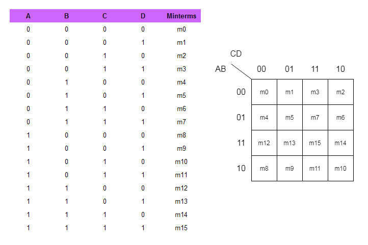
Grouping of cells in a 4-variable K-map
While you minimize a boolean function using 4-variable K-map, group the cell with 1s into 2s, 4s, and 8s, and so on. See the figure below.
Rules for Grouping of cells
Here are some simple rules when group cells.
- Single cells with 1 gives you a term with 4 literals.
- Two adjacent cells will minimize and give you a term with 3 literals.
- A grouping of 4 cells of 1s will give you a term with 2 literals.
- A grouping of 8 cells of 1s will give a single literal.
Therefore, you must always try for maximum number of 1s in a group. Some group overlap each other as we mentioned in earlier in previous post. Each overlapping group must include one uncovered cell that contains a 1. See the figure below to understand this.
4-Variable K-Map Example
In this section, I have given few examples of 4-variable K-maps. For more practice, you can refer to some textbooks with lot of exercises.
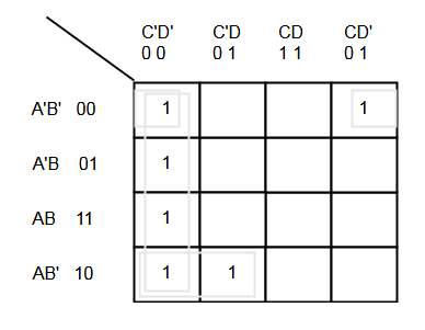
Q1: Minimize the following Boolean function using 4-variable K-map.
F(A,B,C,D) = ∑(0,1,2,4,5,6,8,9,12,13)Solution:
Step 1: Construct a 4-variable K-map and mark all minterms with 1.
Step 2: Look vertically in a selected group and extract any common variable. Also look horizontally, extract any common variable from the group.
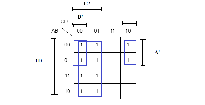
In the group of four, horizontally, you get D’ and vertically, you get A’. Together it is a term of two literal, that is, A’D’. Similarly, the group of 8, vertically everything cancels out and leave just 1 because A’B’ + A’B = A’ and AB + AB’ = A, finally, A’ + A = (1). But, horizontally, for the group of 8, you get C’. Always the group of 8 will give you single literal.
Step 3: Write down all the solution.
Group of 8 = C'
Group of 4 = A'D'
The final expression is F = A'D' + C'
Verify the Solution using Algebraic Method
Let’s verify our solution using Boolean algebraic method.
F(A,B,C,D) = ∑(0,1,2,4,5,6,8,9,12,13)
F = A'B'C'D' + A'B'C'D + A'B'CD' + A'BC'D'+ A'BC'D + A'BCD' + AB'C'D' + AB'C'D + ABC'D' + ABC'D
F = A'B'C'(D' + D) + A'CD'(B' + B) + A'BC'(D' + D) + AB'C'(D'+ D) + ABC'(D' + D)
F = A'B'C' + A'CD' + A'BC' + AB'C' + ABC'
F = A'C'(B' + B) + AC'(B' + B) + A'CD'
F = A'C' + AC' + A'CD'
F = C'(A' + A) + A'CD'
F = C' + A'D' // variable C has no effect hence removed
From the solution above it is clear that the 4-variable K-map is a simple solution to minimize a Boolean function with 4 variables.