So far you have seen, gates and truth table, and output of each gates and combinations of gated circuits. The circuit is represented in the form of a boolean function. Therefore, the process of design starts with deciding:
- number of inputs and outputs
- derive a boolean function that represents the circuit
- minimize the boolean function to obtain a function with minimum number of gates.
The digital design process is to minimize the number of gates by two methods.
- reduce the number of terms in the boolean function.
- reduce the literals or gates from the function.
What are the Methods of Minimizing a Boolean function?
There are three three ways to design boolean circuit.
- Use boolean algebra rules to minimize the circuits
- Use map methods such Karnaugh map, Quine-McClukey tabular method.
- Use software programs suchs VHDL, Verilog, or VSLI and so on.
Since, it is not possible to make a extremely complex circuits with boolean algebra rules or by map methods. Today, we use software programs to design the logic and test the results before implement them as a circuits.
Therefore, for an understanding we can use boolean algebra rules because the software are no different as they also implement there rules to create a circuit design.
Boolean Algebra Rules
Here are the rules for boolean algebra that can be used for minimizing the circuits.
| Boolean Algebra Law | Example |
| Annulment | X + 1 = X , X . 0 = 0 |
| Identity | X + 0 = X , X . 1 = X |
| Idempotent | X + X = X , X . X = X |
| Complement | X + X’ = 1 , X . X’ = 0 |
| Double Negation | (X’)’ = X |
| Commutative | X + Y = Y + X , X . Y = Y . X |
| Associative | X + ( Y + Z) = (X + Y ) + Z , X . ( Y . Z ) = (X . Y ) . Z |
| Distributive | X + ( Y . Z ) = (X + Y ) . ( X + Y ) , X . ( Y + Z ) = X.Y + X.Z |
| DeMorgan’s Theorem | (X + Y)’ = X’ . Y’ , (X . Y)’ = X’ + Y’ |
| Absorbtion | A + A.B = A |
Boolean Minimization Example
In this example, we created a circuit for the function $F = A + A’ \cdot B$ with two gates. See the image below.
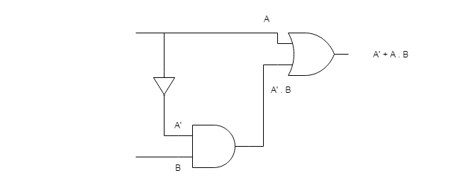
The procedure to minimize the function is given below. You need to apply the rules such that there is less terms and for each term try reducing the variables.
F = A + A'B
= A + AB + A'B   by absorption law A + AB = A
= A + B(A + A')  by distributive law
= A + B(1)       by complement law A + A' = 1
= A + B is the solution
If we design the circuit again and compare the truth table, you will understand why a boolean minimization is necessary.

Truth Table
The truth table of both the functions are given below.
| A | A’ | B | A’ . B | A + A’.B | A + B |
| 0 | 1 | 0 | 0 | 0 | 0 |
| 0 | 1 | 1 | 1 | 1 | 1 |
| 1 | 0 | 0 | 0 | 1 | 1 |
| 1 | 0 | 1 | 0 | 1 | 1 |
The truth table above display output from both the functions and we find that the output is same. In fact, the output A + B is achieves same results with fewer number of gates. Hence, reducing the cost of the circuit.
In the next article, you will learn about representing a boolean function in different forms such as SOP or POS and minimizing boolean function using map methods.